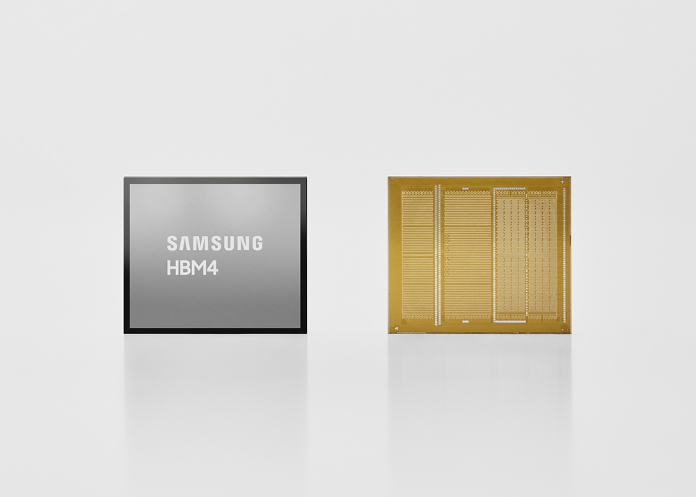
Samsung announced HBM4 mass production and commercial shipments on 12 February 2026. It reported consistent transfer speed of 11.7 Gbps, with capability up to 13 Gbps, using sixth-generation 10nm-class DRAM and a 4nm logic base die. July and October results subsequently reported expanded HBM4 sales.
Samsung made two of its manufacturing businesses part of one product decision. Memory engineers adopted an advanced DRAM process while the foundry supplied the logic underneath the stack. That choice carried more simultaneous process change than simply extending an established design. By the summer, the company was reporting commercial activity on both sides of the arrangement: more HBM4 sales and stronger foundry work around base dies.
Samsung's design put its memory and foundry engineers on the same production programme. The memory business supplied the stacked DRAM; the foundry supplied the advanced logic at its base. February's launch also committed the company to expanding HBM4 capacity and preparing customer-specific memory. As sales grew during the summer, base-die demand became a named contributor to the foundry's recovery. The integrated product was creating work in both operations.
Hwang Chose New Processes Above and Below the Stack
Sang Joon Hwang, head of memory development at the February launch, described a deliberate departure from reusing established designs. His team adopted advanced 1c DRAM and 4nm logic together to create performance headroom for customers. Samsung reported stable yields without an additional redesign. Hwang's decision brought two process-development programmes into one product at the start of its commercial life.
The new interface doubled the number of input/output connections to 2,048. Samsung's 12-layer products offered 24 GB to 36 GB, while a 16-layer route towards 48 GB remained part of the roadmap. More connections also made power delivery and heat management part of the design problem. The company described low-voltage through-silicon connections and an optimised power network, alongside the faster transfer speed.
The finished product sustained 11.7 Gbps transfer speed and could reach up to 13 Gbps. Samsung put maximum bandwidth at 3.3 TB per second per stack. Those characteristics addressed the growing amount of data that AI processors needed to receive. The enlarged interface also increased the engineering work underneath the memory: moving information quickly required the stacked dies and their logic foundation to operate together.
Samsung's reported consistent HBM4 per-pin data-transfer rate in February 2026.
Source 1At GTC, the Stack Became Part of Samsung's Wider Platform Offer
The relationship with NVIDIA had been taking shape before February. Samsung's October 2025 manufacturing announcement described joint HBM4 work alongside memory supply, foundry services and accelerated computing. At GTC in March 2026, Samsung displayed the mass-produced generation and an HBM4E wafer. Its account linked high-performance memory support to NVIDIA's Vera Rubin platform. The commercial launch had become part of a wider presentation to builders of the next AI systems.
Hwang used the event to set out the longer memory roadmap, while Samsung also showed SOCAMM2 for Vera CPUs and its PCIe 6.0 PM1763 SSD. Jensen Huang visited the booth, where Hwang and foundry head Jinman Han appeared alongside him. The collection brought memory, logic manufacturing, packaging and storage into the same customer conversation. HBM4 was the shipping generation at the centre of that display; the HBM4E wafer introduced the next stage.
July's Results Showed the Ramp Reaching More Than the Memory Business
The July results reported that Samsung had scaled HBM4 sales. They also described a record server share of memory revenue, strong prices and capacity constraints. HBM4 was part of an unusually favourable market for server products, including conventional DRAM and enterprise storage.
The foundry account supplied a related development. Samsung attributed a significant improvement in earnings before incentive-related provisions partly to HBM base-die demand, alongside US customer orders. It planned to expand sales of 4nm base-die and language-processing-unit products during the second half. Logic manufacturing was finding AI work through several products, with the memory stack one concrete source of demand.
The same quarter brought HBM4E samples to major customers. February had expected that sampling in the second half of 2026; July's report already described it as completed. That was a dated advance in the next programme, while HBM4 itself was generating sales. Samsung was supporting a commercial generation and moving its successor through customer evaluation at the same time. The two activities were related, but occupied different stages of the product cycle.
By October, Expanded HBM4 Sales Were Accompanied by More Base-Die Work
On 29 October Samsung again reported significantly expanded HBM4 sales. The foundry business also reported improved revenue and earnings supported by HBM base-die growth and advanced-node business. The February manufacturing choice was now visible across two reporting periods: memory sales were expanding, while production of the logic underneath those stacks supported another operation within the group.
Samsung's next sales strategy kept HBM, server DRAM and SSDs together, with more multi-year customer contracts planned for 2027. Strong server demand and rising market prices had accompanied the HBM4 ramp. Within that broader upturn, the product had delivered the continuation that mattered to February's decision: a new stack in customers' systems, repeat expansion of sales and more manufacturing work for the foundry that helped make it.
DSML research · 8 October 2026 · Revised 31 October 2026